*************************************************************************************************************************
OSOYOO
Introduction of OSOYOO Universal IO Breakout Board
Model: OSOYOO Universal IO Breakout Board | Version 1.0
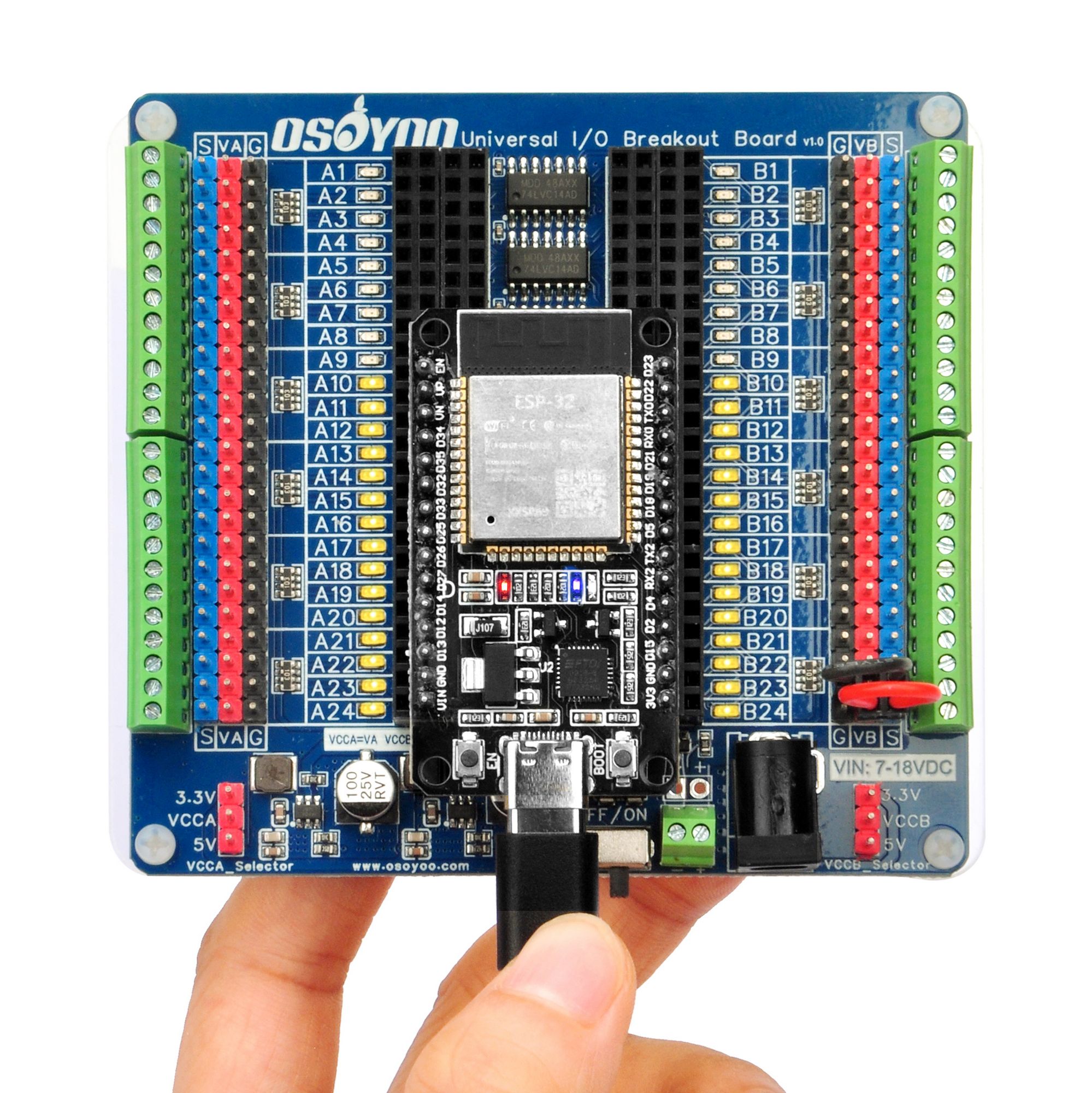
Fig 1 – OSOYOO Universal IO Breakout Board with an ESP32 module inserted
1. Overview
The OSOYOO Universal IO Breakout Board is a versatile GPIO expansion and debugging platform designed to accelerate hardware prototyping with virtually any MCU development board. Unlike fixed-format breakout boards that only work with one specific module, this board features two sets of 2×24P female pin-header sockets that accept MCU modules with a pin row spacing of 0.6 / 0.7 / 0.8 / 0.9 / 1.0 / 1.1 / 1.2 inch, making it compatible with Arduino Nano, ESP32 variants, ESP8266 NodeMCU, Raspberry Pi Pico, and many others. All pin headers use the standard 2.54 mm pitch.
A key feature is the per-pin LED status indicator: every GPIO pin on both socket sides has a dedicated LED that turns ON when the pin is driven HIGH and OFF when LOW. The LEDs are driven by an on-board 74LVC14AD hex Schmitt-trigger inverter, electrically isolated from the MCU GPIO — so the indicators add no load, do not affect ADC accuracy, and do not disturb open-drain buses (I²C, 1-Wire) or ESP32 strapping pins during boot.
Two on-board JW5357MSOTB#TR DC-DC step-down converters generate two fixed source voltages — one 5 V and one 3.3 V (up to 3 A each). The VCCA_Selector and VCCB_Selector jumpers then route the VA and VB rails to either the 3.3 V or the 5 V source, so each rail can be set independently to 3.3 V or 5 V — the two rails may be the same voltage or different. An SI2302 reverse-polarity protection MOSFET, on-board power switch, barrel-jack, and screw-terminal input complete the power system.
2. Target Applications
| Application Area |
Typical Projects |
| Robot & Smart Car Control |
2WD / 4WD robot cars, tank chassis, mecanum-wheel platforms, line-following robots, obstacle-avoidance cars, servo-steered vehicles |
| Sensor Integration |
Temperature / humidity (DHT11/22), ultrasonic ranging (HC-SR04), infrared detection, color sensing, soil moisture |
| Motor & Actuator Driving |
RC servo control, DC motor PWM via external driver (L298N, DRV8833), stepper motor stepping, relay switching |
| IoT & Wireless Projects |
Wi-Fi / BLE sensor nodes (ESP32 / ESP8266), MQTT data logging, remote monitoring dashboards |
| Display & User Interfaces |
OLED / LCD experiments, button matrices, buzzer alarms, RGB LED strips |
| Education & Prototyping |
Learning GPIO, I²C / SPI / UART protocols, ADC sampling, PWM generation, interrupt handling — no breadboard needed |
| Hardware Debugging |
Real-time pin-state visualization; verify firmware behavior without a logic analyzer or oscilloscope |
3. Features
- ✔ Universal MCU Compatibility — Two sets of 2×24P (48-pin) female sockets accept MCU boards with 0.6 / 0.7 / 0.8 / 0.9 / 1.0 / 1.1 / 1.2 inch pin-row spacing, covering most popular development boards.
- ✔ Per-Pin LED Status Indicators — Every GPIO pin on both socket sides has an individual LED reflecting real-time HIGH / LOW state. ON = HIGH, OFF = LOW.
- ✔ Non-Intrusive LED Drive Circuit — 74LVC14AD hex Schmitt-trigger inverters drive the LEDs, not MCU GPIO directly. Zero impact on GPIO load, ADC accuracy, I²C / SPI bus integrity, or boot strapping pins.
- ✔ Floating IO Warning — A floating (high-impedance) GPIO may partially illuminate its LED. This helps developers spot unconfigured pins at a glance.
- ✔ Reverse Polarity Protection — SI2302 N-channel MOSFET prevents damage when DC power polarity is accidentally reversed.
- ✔ Dual Selectable Power Rails (VA & VB) — Two on-board JW5357MSOTB#TR converters provide a fixed 5 V source and a fixed 3.3 V source (up to 3 A each). The VA and VB rails are independently routed to either source, so each can be 3.3 V or 5 V.
- ✔ Selectable Rail Voltage (3.3 V / 5 V) — VCCA_Selector and VCCB_Selector jumpers set each rail independently. Default: 3.3 V. Each rail must be set to one voltage only.
- ✔ Dual Peripheral Connection Options — Each GPIO row provides a 2.54 mm pin header and a screw terminal (S / V / G) for sensors, servos, and peripherals.
- ✔ Wide DC Input Range — 7–18 V DC via 5.5×2.1 mm barrel jack or screw terminal. Automatic DC / USB power switching on MCU power path.
- ✔ On-Board Power Switch — Slide switch enables / disables the VA / VB DC-DC outputs.
- ✔ USB Power Support — When using only MCU USB power, remove VA/VB Selector jumpers and connect VA/VB/GND correctly to prevent DC-DC backflow.
4. Technical Specifications
| Parameter |
Value / Description |
| MCU Socket Type |
2×24P female pin headers × 2 (A side left + B side right) |
| Compatible MCU Width |
0.6 / 0.7 / 0.8 / 0.9 / 1.0 / 1.1 / 1.2 inch (pin row spacing) |
| Pin Pitch |
2.54 mm (0.1 inch), standard |
| Max MCU Pins Supported |
48 total (24 per side) |
| LED Indicator Driver IC |
74LVC14AD — hex inverter with Schmitt-trigger inputs (SOIC-14) |
| Number of LED Indicators |
Up to 48 (one per socket pin, A1–A24 and B1–B24) |
| Reverse Polarity Protection |
SI2302 N-Channel MOSFET |
| DC-DC Converters |
JW5357MSOTB#TR × 2 — one fixed 5 V source, one fixed 3.3 V source |
| VA Rail Output Voltage |
3.3 V or 5 V — VCCA_Selector routes VA to the 3.3 V or 5 V source; default 3.3 V |
| VB Rail Output Voltage |
3.3 V or 5 V — VCCB_Selector routes VB to the 3.3 V or 5 V source; default 3.3 V |
| Max Output Current |
3 A per converter (5 V total ≤ 3 A and 3.3 V total ≤ 3 A; the limit is shared when both rails select the same voltage) |
| DC Input Voltage |
7–18 V DC |
| DC Input Connector |
5.5×2.1 mm barrel jack (center positive) + screw terminal |
| Peripheral Headers (per row) |
S / V / G — 2.54 mm 3-pin header + screw terminal |
| Power Switch |
Slide switch (enables / disables VA / VB DC-DC output) |
| PCB Color |
Blue, ENIG finish |
| Board Dimensions |
Approx. 120 mm × 115 mm (see Mechanical section) |
5. Board Layout & Components
5.1 Front View
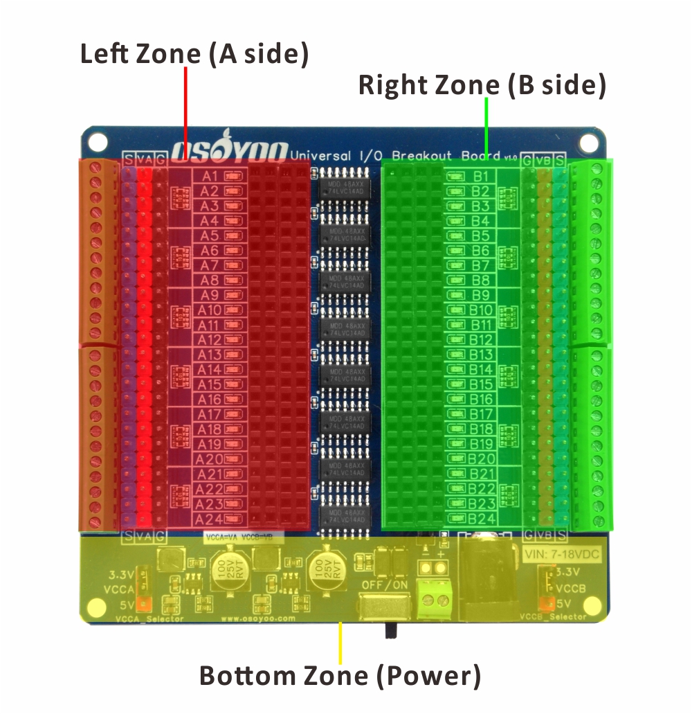
Fig 2 – Front 2D PCB layout (A side left, B side right, power section bottom)
The board is divided into three zones:
- Left Zone (A side): MCU socket pins A1–A24, column order from outer to inner — S (signal header), V (VA power), A (MCU socket pin), G (GND). LED indicators sit adjacent to the A column.
- Right Zone (B side): MCU socket pins B1–B24, column order from inner to outer — G (GND), B (MCU socket pin), V (VB power), S (signal header). LED indicators sit adjacent to the B column.
- Bottom Zone (Power): Two DC-DC converters (one fixed 3.3 V, one fixed 5 V), ON/OFF switch, DC barrel jack, VIN screw terminal, VCCA_Selector jumper (bottom-left), VCCB_Selector jumper (bottom-right).
5.2 Back View & Silkscreen Notes
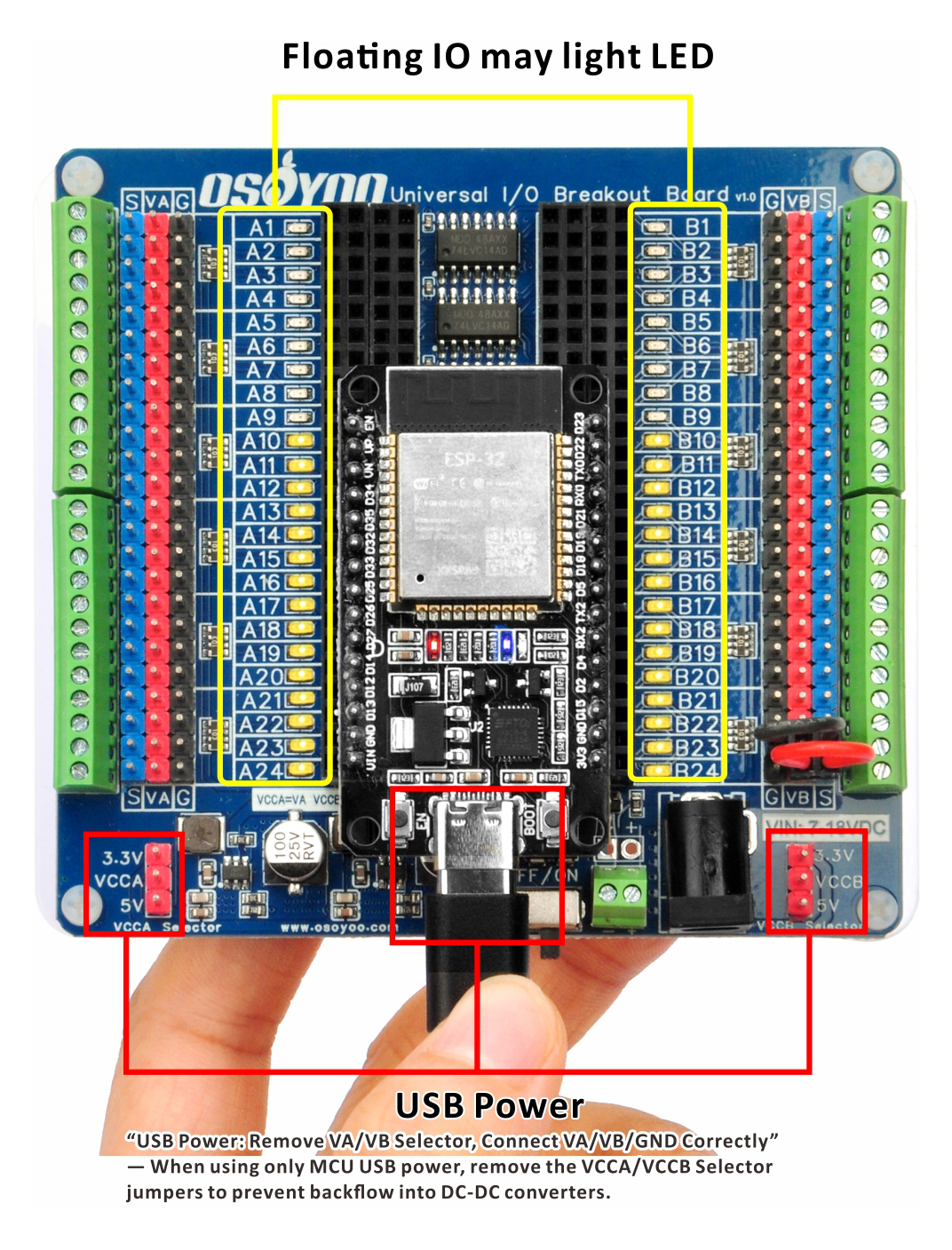
Fig 3 – Back 2D PCB layout showing usage reminders printed on silkscreen
Key reminders printed on the back silkscreen:
- “Floating IO may light LED!” — A floating GPIO may partially activate its LED. Always define pin modes in code.
- “USB Power: Remove VA/VB Selector, Connect VA/VB/GND Correctly” — When using only MCU USB power, remove the VCCA/VCCB Selector jumpers to prevent backflow into DC-DC converters.
- “7-18V DC Input” — DC barrel jack input range.
- “0.6–1.2″ Pitch Support” — MCU socket width compatibility range.
- “VA/VB Indep rails (Jumper for 3.3V/5V)” — VA and VB are fully independent; each has its own selector.
- “VA/VB: ONE VOLTAGE ONLY” — Each selector must bridge to either 3.3 V or 5 V, never both simultaneously.
- “Output 3A Max” — Maximum current per DC-DC converter output.
5.3 Component Descriptions
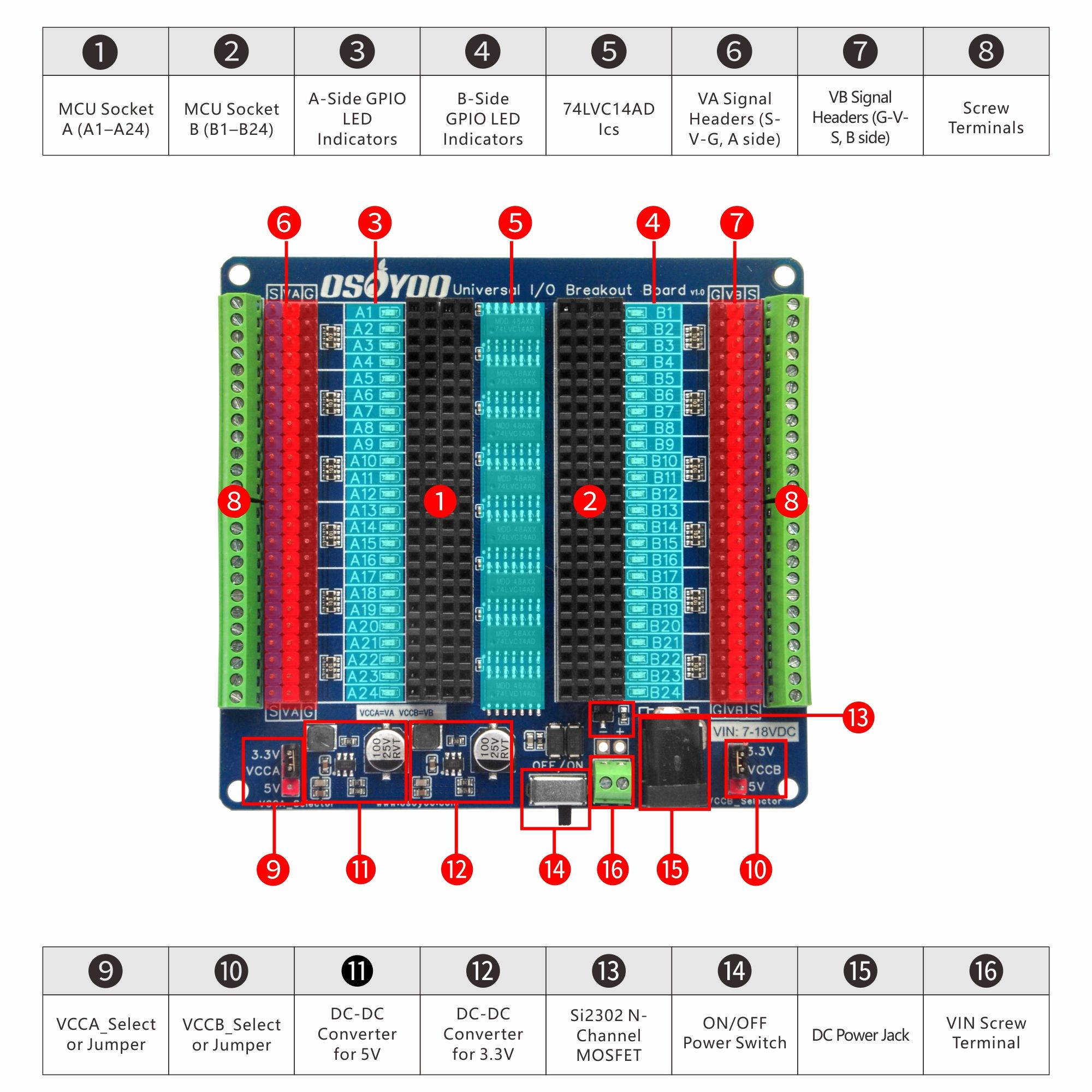
Fig 4 – PCB component layout render
| No. |
Component |
Description |
| ① |
MCU Socket A (A1–A24) |
Left-side 2×24P female pin header. Accepts the left-column pins of the MCU board. Row A1 = topmost pin. |
| ② |
MCU Socket B (B1–B24) |
Right-side 2×24P female pin header. Accepts the right-column pins of the MCU board. Row B1 = topmost pin. |
| ③ |
A-Side GPIO LED Indicators |
24 LEDs showing real-time HIGH (ON) / LOW (OFF) state of each A-side MCU pin. |
| ④ |
B-Side GPIO LED Indicators |
24 LEDs showing real-time HIGH / LOW state of each B-side MCU pin. |
| ⑤ |
74LVC14AD ICs |
Hex Schmitt-trigger inverter ICs. Drive LED indicators without drawing current from MCU GPIO pins. Multiple ICs cover all 48 indicator positions. |
| ⑥ |
VA Signal Headers (S-V-G, A side) |
3-pin 2.54 mm headers: S = MCU GPIO signal, V = VA rail power, G = GND. Connect sensors, servos, or modules here. |
| ⑦ |
VB Signal Headers (G-V-S, B side) |
3-pin 2.54 mm headers: G = GND, V = VB rail power, S = MCU GPIO signal. Same purpose as ⑥ for B-side peripherals. |
| ⑧ |
Screw Terminals |
Screw-clamp connectors alongside each S/V/G row for secure, tool-free wire connections. |
| ⑨ |
VCCA_Selector Jumper |
Bottom-left 3-pin jumper. Routes the VA rail to the 3.3 V or the 5 V source. Default: 3.3 V. |
| ⑩ |
VCCB_Selector Jumper |
Bottom-right 3-pin jumper. Same function as ⑨ for the VB rail. Default: 3.3 V. |
| ⑪ |
DC-DC Converter (fixed output) |
JW5357MSOTB#TR step-down converter. One of the two on-board converters; the pair produces a fixed 5 V source and a fixed 3.3 V source from the 7–18 V input (up to 3 A each). Check the silkscreen for which converter is which. |
| ⑫ |
DC-DC Converter (fixed output) |
The second JW5357MSOTB#TR. The VCCA_Selector and VCCB_Selector (⑨ / ⑩) then route the VA / VB rails to either the 3.3 V or the 5 V source. |
| ⑬ |
SI2302 N-Channel MOSFET |
Reverse polarity protection. Prevents current flow if DC input polarity is accidentally reversed, protecting all board components. |
| ⑭ |
ON/OFF Power Switch |
Slide switch controlling VA and VB DC-DC output. Switching OFF cuts peripheral power; does not cut MCU USB power. |
| ⑮ |
DC Power Jack |
5.5×2.1 mm barrel jack, center positive. Input: 7–18 V DC from adapter or bench supply. |
| ⑯ |
VIN Screw Terminal |
Alternative DC input (+ / −). Same 7–18 V range as the barrel jack; useful when connecting via wire leads. |
6. Power Configuration
6.1 External DC Power (7–18 V) — Recommended for Full Operation
1
Connect a 7–18 V DC supply to the barrel jack (center positive) or VIN (+/−) screw terminal.
2
Set VCCA_Selector to the desired VA voltage (3.3 V or 5 V). Repeat for VCCB_Selector. Default is 3.3 V for both.
3
Switch the ON/OFF switch to ON. The VA / VB rails are now powered.
4
Insert the MCU board into the socket. Connect the MCU’s power pin(s) to the corresponding V and GND rails via a 2-pin jumper cap or female-to-female wire (see MCU-specific tutorial pages).
⚠ Important: Before connecting any peripheral, confirm the VCCA / VCCB voltage selection matches the peripheral’s logic level. Some sensors operate at 3.3 V only and will be damaged by 5 V.
6.2 USB Power from MCU Board — LED Indicator Operation
When only USB power is available (e.g., connected to a computer for programming), the DC-DC converters are inactive. To power the LED indicators from the MCU’s USB supply:
1
Remove both the VCCA_Selector and VCCB_Selector jumper caps.
2
Connect the MCU board’s USB-powered 3.3 V or 5 V output pin to the VA or VB rail V-header using a female-to-female wire. This feeds the MCU’s USB supply into the indicator IC power rail.
3
Ensure GND is common between the MCU and the breakout board.
⚠ Critical: If the VCCA / VCCB Selector jumpers remain in place while USB power is active, reverse current will flow back into the DC-DC converter circuits through the selector, potentially damaging the converters. Always remove the selector jumpers when operating in USB-only mode.
Note: VA and VB rails are independent. If the MCU’s power pin is only on one side, the other side’s V rail has no power in USB mode. Connect the powered side’s V-header to the unpowered side’s V-header with a jumper wire, or run a wire from the MCU’s power S-header to that side.
6.3 VA / VB Rail Voltage Selection
| Jumper |
Rail |
3.3 V Position |
5 V Position |
Default |
| VCCA_Selector |
VA (A side) |
Bridge center ↔ 3.3 V pad |
Bridge center ↔ 5 V pad |
3.3 V |
| VCCB_Selector |
VB (B side) |
Bridge center ↔ 3.3 V pad |
Bridge center ↔ 5 V pad |
3.3 V |
⚠ One Voltage Only: Never bridge both 3.3 V and 5 V pads on the same selector simultaneously. Each rail supports only one voltage at a time.
7. Important Notes
- Floating GPIO Pins: An unconfigured (floating) GPIO may cause its LED to glow dimly or flicker. Always call
pinMode(pin, OUTPUT) or pinMode(pin, INPUT_PULLUP) to define a stable state.
- MCU Power Pin Connection: Unlike fixed-format breakout boards, the MCU’s VCC and GND pin positions vary by board model. You must connect the MCU’s power pin(s) to the V and G rails manually (jumper cap or wire) before the MCU can receive power from the breakout board’s DC supply. See each MCU tutorial page for specifics.
- VA and VB Are Independent: A-side pins (A1–A24) are powered by VA; B-side pins (B1–B24) by VB. If all power pins are on one side, the other side’s V rail may have no power. Bridge between sides as needed.
- Maximum Input Voltage: Do not exceed 18 V on the VIN input. Higher voltage may damage DC-DC converters and other components.
- Minimum Input Voltage: A minimum of 7 V is required for correct DC-DC regulation. Input below 7 V results in unstable or incorrect output.
- Per-Converter Current Limit: The 3.3 V and 5 V sources are each rated 3 A. Because both rails draw from these two shared converters, if VA and VB are set to the same voltage their combined current must stay within that one converter’s 3 A; if set to different voltages each has its own 3 A.
- Confirm Voltage Before Connecting Peripherals: Applying 5 V to a 3.3 V-only sensor can permanently damage it. Verify the selector position first.
- LED Indicator Behavior:
| GPIO State |
LED Indicator |
| Output HIGH |
LED ON (solid) |
| Output LOW |
LED OFF |
| Floating / High-Z |
LED may glow dimly or flicker |
| Input with pull-up |
LED ON |
| Input with pull-down |
LED OFF |
8. Mechanical Information
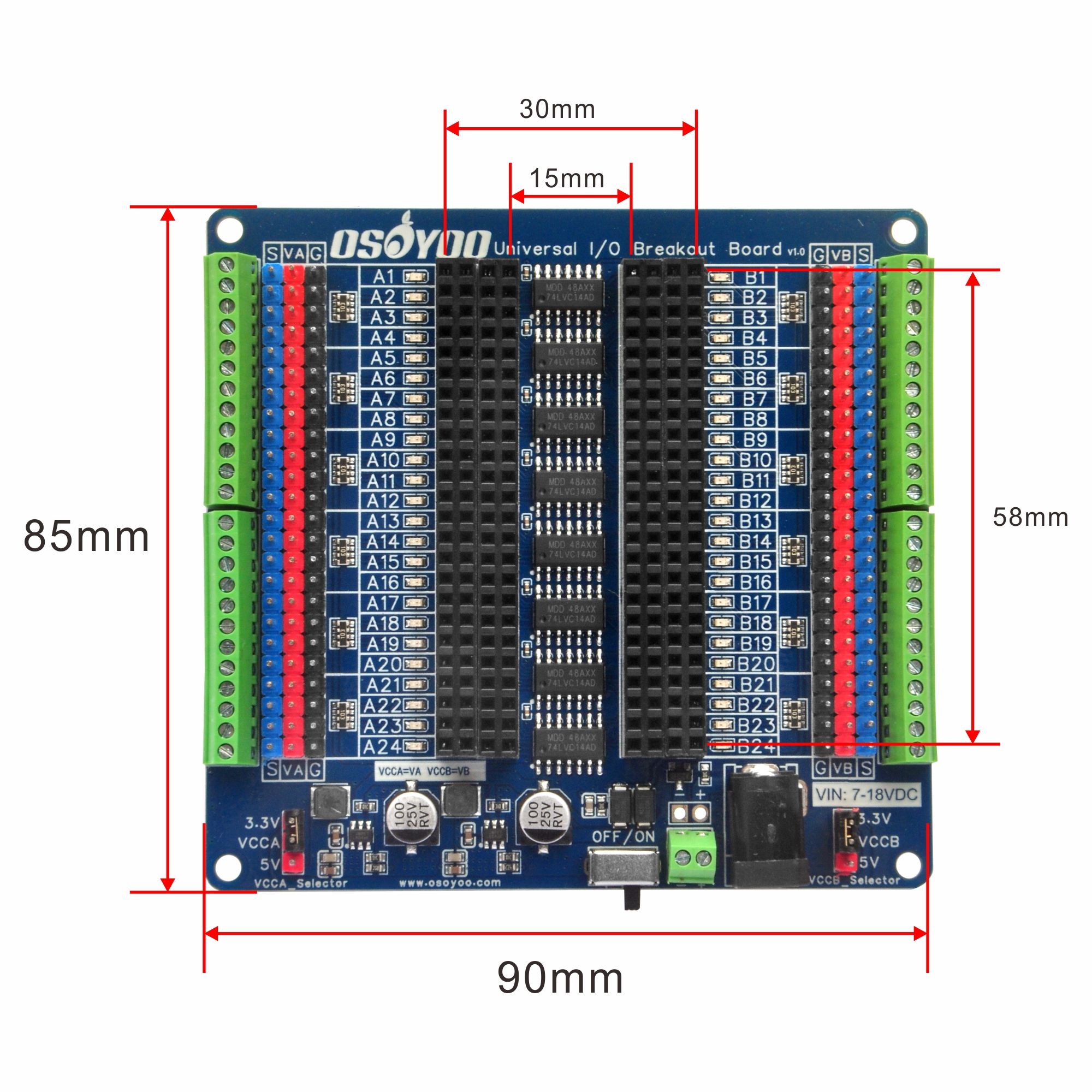
Fig 5 – Back view showing PCB outline
| Parameter |
Value |
| PCB Dimensions |
Approx. 90 mm × 85 mm |
| Mounting Holes |
4 × M3 (one at each corner) |
| Mounting Hole Diameter |
3.2 mm |
| PCB Thickness |
1.6 mm |
| PCB Color |
Blue, ENIG finish |
| Board Weight |
Approx. 55 g (without MCU board) |
Note: Exact dimensions should be confirmed against the current production drawing. Values above are approximate.
9. Related Documents
| Document |
File |
| Schematic Diagram |
原理图SCH_OSOYOO Universal IO Breakout Board_2026-05-14.png |
| Front PCB 2D Drawing |
正面PCB-2D_PCB1_2026-04-09.png |
| Back PCB 2D Drawing |
底面2D_Universal IO Breakout Board.png |
| PCB Layout Render |
PCB_PCB1_2026-05-13 (1).png |
| 74LVC14AD Datasheet |
Hex inverter with Schmitt-trigger inputs — NXP / TI |
| SI2302 Datasheet |
N-channel MOSFET — reverse polarity protection |
| JW5357MSOTB#TR Datasheet |
DC-DC step-down converter |
MCU Tutorial Pages
ESP32
Arduino Nano
Raspberry Pi Pico
ESP8266 NodeMCU
Other Boards
OSOYOO Related Products
MCU Debug Shield Series
38P ESP32 Breakout
Nano Breakout Board
30P ESP8266 Breakout